RESONAC (Semiconductor Materials Manufacturer in Japan) to Use Virtual Reality Technology for Product Development
— Enables engineers to experience “molecular level visualization,” and makes a significant contribution to accelerating development and discovery of new materials —
Resonac Corporation (TOKYO: 4004) (President: Hidehito Takahashi) has successfully applied virtual reality (VR) technology*1 to the development of semiconductor materials. This is the first time that the VR technology has been implemented to develop semiconductor materials in Japan*2.
Molecular dynamics (MD) simulation*3 is a powerful tool for R&D of semiconductor materials at the atomic scale. We employ MD simulations to study interactions at the interface between different materials, such as the adsorption and adhesion of organic molecules on an inorganic substrate with thousands of atoms. However, their behaviors are hard to observe on a simple computer screen. As a result, even experts in computational science often perform only a statistical analysis. The analysis is not easy for non-experts to understand.
Six months ago, we began exploring VR technology with head-mounted display*4 for analyzing the behavior of molecules at interfaces in three-dimensions. The technology visualizes “the atomic and molecular world” of 0.1 nm, one ten-billionth of a meter, in front of our eyes, allowing us to place ourselves at the same scale. We can observe the molecular behavior at the substrate-molecule interface while intuitively handling “molecules”.
We also found that the VR technology is helpful for non-experts to understand the behaviors, such as how atoms in a substrate bond with molecular chains of organic molecules. The VR technology, thus, facilitates communication between computational science and materials development experts, accelerating our R&D activities.
Our first application of VR technology is in “analyzing the mechanisms of interaction between an inorganic substrate and organic molecules” for semiconductor and electronic materials, such as CMP slurries (polishing materials)*5.
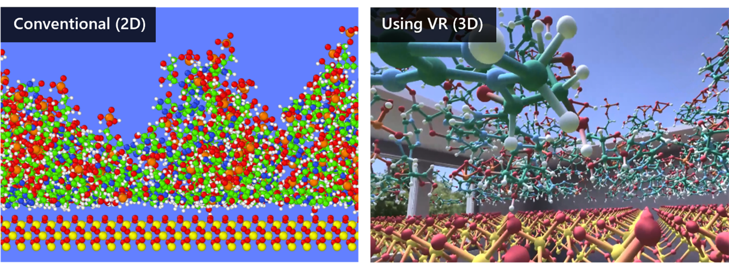
Comparison of a conventional image represented in two-dimensions, and an image visualized using VR represented in three-dimensions
Note: These are examples based on MD simulations of inosinic acid (C10H13N4O8P) on a silica (SiO2) substrate, and are not actual examples in the fields of semiconductor and electronic materials.
Note: The image where VR is used is a two-dimensional representation of material originally represented in three-dimensions. When viewed on a head-mounted display, viewers can clearly experience positional relationships in a more spatial way.
View a video of VR in use here: https://youtu.be/7E5YjA7xxf0
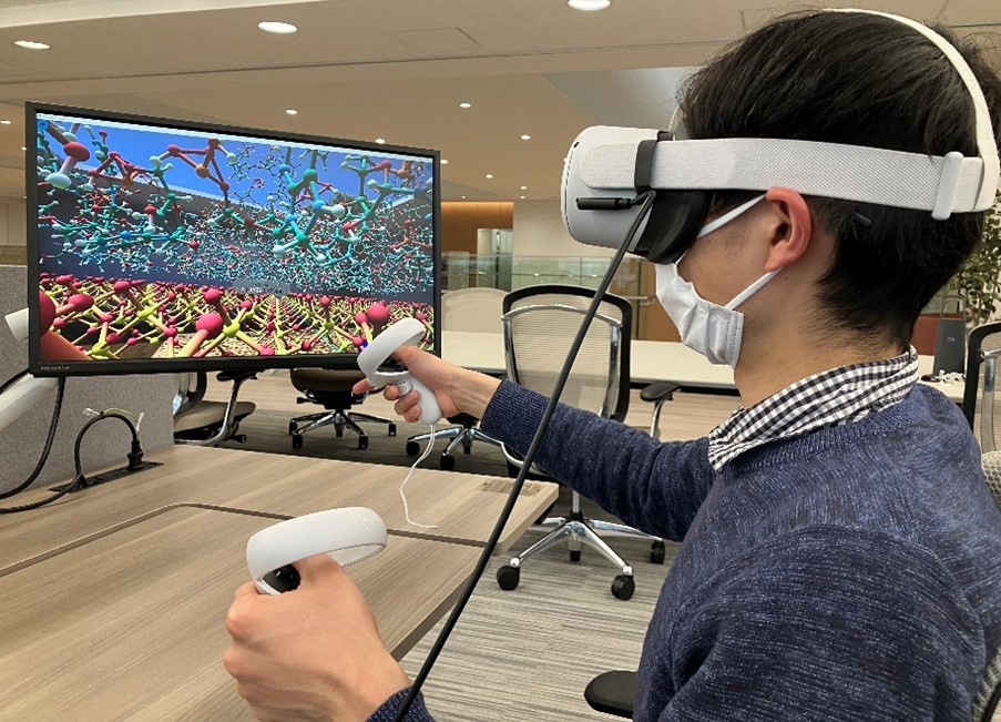
An engineer using VR with a head-mounted display
Dr. Yoshishige Okuno, Head of Research Center for Computational Science and Informatics, Resonac Corporation, said “VR technology greatly supports our R&D based on computational molecular-design. It leverages our advanced computational science technology to help more in-depth analysis and discovery of new materials. We would like to firstly extend the VR throughout the company, and to secondly elevate it to an internal infrastructure. We will fully utilize computational science and simulations to accelerate our research and development.”
*1 VR technology: VR stands for Virtual Reality, a technology that allows users to experience computer-generated digital spaces as if they were real.
*2 Based on Resonac’s survey.
*3 Molecular dynamics simulations: A method of calculation for analyzing the behavior of molecules by focusing on the motion of atoms and solving equations of motion that take into account the interactions between atoms. It is also referred to as molecular simulation.
*4 Head-mounted display: A display device worn on the head that uses the parallax between the left and right eyes to display virtual reality in three-dimensions.
*5 CMP slurry: CMP (Chemical Mechanical Planarization) slurry is a material consisting of abrasive grains and liquid for polishing and planarizing unevenness generated in the circuit formation process of semiconductor devices.